- Optical AI breakthrough: University of Florida researchers have developed a first-of-its-kind photonic computer chip – the first to put optical computation directly on-chip for neural networks – that uses light (lasers and microscopic lenses) instead of electricity to perform one of AI’s most power-intensive tasks news.ufl.edu.
- 100-fold energy efficiency gain: Using light dramatically cuts the power needed for key AI computations. The prototype achieved 10× to 100× greater energy efficiency than current electronic chips performing the same operations news.ufl.edu, effectively running these calculations at “near zero energy,” according to the lead researchers news.ufl.edu.
- No loss in accuracy: In tests, the photonic chip’s performance matched traditional processors – it correctly classified images of handwritten digits with ~98% accuracy, virtually indistinguishable from a normal digital neural network, while consuming only a tiny fraction of the energy news.ufl.edu, allaboutcircuits.com.
- How it works: The chip uses laser light and tiny lenses to do math. It converts input data (for example, pixel values from an image) into laser light on the chip. That light then passes through two sets of minuscule Fresnel lenses – flat micro-lenses narrower than a human hair – which perform a convolution (pattern-matching calculation) by bending and combining the light. Finally, the resulting light pattern is converted back into an electronic signal to complete the AI computation news.ufl.edu, sciencedaily.com.
- Parallel processing with photons: Unlike conventional chips, the photonic design can handle many operations simultaneously. By using lasers of different colors (a technique called wavelength multiplexing), the chip processes multiple data streams in parallel through the same optical lens system – massively boosting throughput without extra energy or size penalty sciencedaily.com, news.ufl.edu.
- Big impact on AI’s future: By slashing AI’s power requirements by orders of magnitude, this photonic chip paves the way for greener, faster AI. It could help relieve the strain that energy-hungry AI workloads put on power grids news.ufl.edu and enable advanced AI to run in many new settings – from cloud data centers down to tiny edge devices like drones, wearables, or even medical implants, which previously couldn’t handle such tasks due to power and heat constraints allaboutcircuits.com.
A Chip That Computes with Light (and Why It’s a Big Deal)
Artificial intelligence has become ubiquitous, powering everything from facial recognition to real-time language translation – but this progress comes at a steep cost in power consumption sciencedaily.com. In particular, convolutional neural networks (CNNs), which drive many of AI’s “greatest hits” (like spotting faces in photos, reading handwriting, or translating text), chew through enormous computing resources by scanning data with millions of tiny filters to detect patterns newatlas.com. Performing these convolutions is so intensive that it’s been likened to “running a marathon through every pixel” of an image newatlas.com. As AI models grow more complex, the energy and time required for such calculations have become a serious bottleneck, fueling concerns about efficiency and even talk of an impending “AI recession” if costs keep skyrocketing newatlas.com.
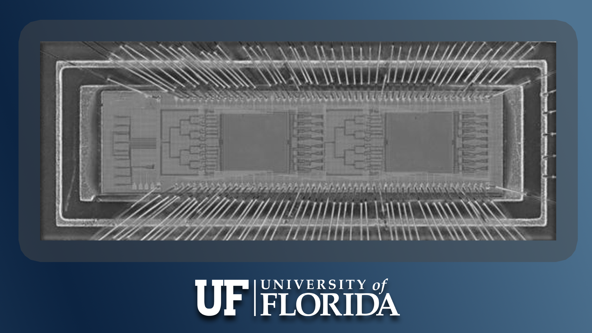
To tackle this challenge, researchers at the University of Florida built something radical: a new chip that swaps electricity for light to handle one of AI’s most power-hungry operations newatlas.com. Their prototype, officially called a photonic joint transform correlator (pJTC), uses beams of laser light and on-chip optical components to perform convolution – the core pattern-finding step in vision and language tasks – in a fraction of the time and energy that traditional silicon chips require news.ufl.edu. In essence, the chip is doing math with photons instead of electrons.
Here’s how it works: Data (for example, an image or any numerical input) is first encoded into pulses of laser light on the chip itself. These light-encoded data then pass through microscopic Fresnel lenses integrated on the silicon. Fresnel lenses are ultra-flat lenses (similar to the kind in lighthouse lamps, but shrunken to a few microns across) that can bend and focus light efficiently news.ufl.edu. As the light beams carrying the data go through the two sets of tiny lenses, they optically perform the convolution operation – essentially overlaying and correlating the data with a filter pattern by means of light interference. Once this optical calculation is done (in a literal flash of light), the resulting light pattern is converted back into an electronic signal that conventional computer circuits can read news.ufl.edu, sciencedaily.com. The entire process happens at light-speed and with almost no resistive energy loss, since photons, unlike electrons, don’t dissipate energy as heat when traveling through the optical medium.
Crucially, this light-based approach doesn’t sacrifice accuracy or capability. In a proof-of-concept demonstration, the team integrated their photonic convolution unit into a simple neural network and used it to recognize handwritten digit images (the classic MNIST benchmark test). The optical chip handled the task just as accurately as a standard digital processor – about 98% accuracy in classifying the digits, which is on par with existing AI models news.ufl.edu. The difference is that the photonic chip did so while consuming dramatically less power. One analysis showed it could reduce the energy per inference (each classification) by about 100× compared to an electronic chip, operating at near “picojoules” of energy per operation (that’s one-trillionth of a joule) allaboutcircuits.com. In other words, it’s performing meaningful AI tasks at practically zero energy cost. “Performing a key machine learning computation at near zero energy is a leap forward for future AI systems,” said Volker J. Sorger, the University of Florida professor who led the study news.ufl.edu. This leap in efficiency, he noted, is “critical to keep scaling up AI capabilities in years to come” news.ufl.edu – a sentiment echoing the broader industry’s quest to rein in power consumption so that AI can continue to grow.
Not only is it efficient, it’s also the first time engineers have achieved this level of optical computing integration. “This is the first time anyone has put this type of optical computation on a chip and applied it to an AI neural network,” explained Dr. Hangbo Yang, a research associate professor on the UF team news.ufl.edu. In other words, while optical computing concepts have been explored for decades, this marks a milestone: a self-contained photonic computing module working within a neural network system. By proving that lasers and lenses can be monolithically built into a chip to do AI math, the team has opened a new frontier for how we might build future AI hardware.
How Is a Photonic Chip Different from a Traditional Chip?
This photonic AI chip departs from conventional computer chips in several important ways:
- Computing with light vs. electricity: Ordinary processors rely on electrical transistors switching electrons on and off. In the new design, laser-generated photons carry and process information instead news.ufl.edu. Because light can travel through optical materials with minimal resistance, the computation generates far less heat and loses virtually no energy inside the chip. The heavy lifting (the multiply-accumulate operations in convolution) is done by the physics of light interference, rather than by masses of transistors flipping states.
- Massively parallel operations: In electronic chips, doing many operations in parallel is limited by chip area and complex wiring; each additional processing core or circuit multiplies power usage. In the photonic chip, multiple data channels can be processed simultaneously using different wavelengths (colors) of laser light without needing duplicate hardware allaboutcircuits.com. Several light beams of different colors can pass through the same lens system at once without interfering, performing many convolutions in parallel. This wavelength-division multiplexing gives huge throughput gains – the prototype can handle streams in parallel on one tiny optical setup allaboutcircuits.com – which would be difficult for a traditional chip unless it were much larger and more power-hungry.
- Ultra-low energy and heat: Perhaps the biggest difference is efficiency. Photonic processing essentially eliminates the major sources of energy loss (like resistive heating in wires and transistors). The UF team’s chip demonstrated a 100-fold reduction in energy per inference compared to state-of-the-art electronic approaches allaboutcircuits.com. In practical terms, it operates on the order of femtojoules or picojoules per operation, whereas today’s AI accelerators might use nanojoules or more. Such a drastic cut in power means the chip runs cool and could even be powered by small batteries or energy harvesting in environments where normal chips would quickly drain the power supply. It’s a fanless, “near-zero-power” computing paradigm allaboutcircuits.com, which also means it can be packed densely without overheating.
- A hybrid computing model: Interestingly, the photonic chip doesn’t have to work alone – it is designed to integrate with conventional electronics. In the current prototype, the optical module handles the convolution layer of a neural network, and the remaining layers (like the decision-making neurons) run on regular digital circuits allaboutcircuits.com. This kind of hybrid system lets optics do what it does best (fast, energy-free parallel math) and leaves other tasks (logic, memory storage, nonlinear operations) to traditional silicon. The result is a new compute model where a photonic accelerator sits alongside CPUs/GPUs. Future AI hardware might co-pack photonic convolution units with electronic logic and memory on the same chip or module allaboutcircuits.com. This compatibility is key – the optical chip was made with standard silicon fabrication techniques allaboutcircuits.com, meaning it could be scaled up and combined with existing semiconductor technology relatively seamlessly, rather than requiring exotic materials or huge free-space optical setups.
In short, by using photons instead of electrons, the new chip achieves a combination of high parallelism, low energy per operation, and integration potential that sets it apart from conventional processors. This doesn’t mean electronic chips will disappear – instead, we’re likely looking at a future where photonic and electronic components work together, each handling the aspects of AI computation they’re best suited for.
Transforming AI: Why Does This Matter?
The advent of an efficient photonic AI chip could be a game-changer for the field of artificial intelligence, especially as we hit walls in power and scaling with existing hardware. Today’s cutting-edge AI models (from large language models to advanced vision systems) devour electricity – so much so that power bills and cooling demands are becoming limiting factors for AI research and deployment sciencedaily.com. “AI systems…consume vast amounts of electricity,” noted a report on the UF chip, underscoring the sustainability challenges of current AI growth sciencedaily.com. Data centers running AI workloads are straining power grids and pumping out heat, to the point that some experts worry about an “AI energy crisis.” In fact, rising compute costs have sparked concerns of an “AI recession,” where innovation could slow because running ever-bigger models simply becomes too expensive or energy-prohibitive newatlas.com.
This is why a 100× efficiency boost is such a big deal. By dramatically cutting the energy per computation, photonic chips could remove a major bottleneck for AI progress. Tasks that used to gulp down kilowatts might only sip milliwatts. For AI at scale, that means much lower operating costs and carbon footprint in the cloud. For example, large model training or massive cloud inference services could be made far more sustainable – potentially saving huge amounts of electricity (and reducing the need for giant cooling systems in data centers) if optical accelerators take on the heavy lifting of neural network math news.ufl.edu. The UF team’s chip, for instance, has been measured at up to 305 trillion operations per second per watt of power – an astronomical throughput per energy rate that “leaves traditional chips in the dust,” as one tech outlet put it newatlas.com. This kind of efficiency can translate to performing the same AI task with only ~1% of the energy that would normally be required, a leap that would greatly trim the electricity bills of AI-heavy organizations and cut the emissions associated with AI computation.
Energy efficiency isn’t the only benefit; speed and capability go up as well. Since the photonic chip can do so many operations in parallel (and doesn’t overheat when pushed hard), it can accelerate AI tasks in real time. An optical convolution that might have taken a significant amount of time on a CPU or even GPU can be done almost instantaneously as light passes through a lens. This means faster processing and lower latency for AI applications. Models that were too slow to run on low-power devices might now run fluidly. And by alleviating the power and thermal constraints, we can also pack more AI computing into smaller devices or scale up AI in the cloud without a proportional increase in cooling and energy infrastructure.
Ultimately, innovations like this photonic chip could change the trajectory of AI development. “In the near future, chip-based optics will become a key part of every AI chip we use daily,” predicts Professor Sorger, envisioning a new norm of hybrid optical-electronic computing news.ufl.edu. By making core computations essentially free (in energy terms), such technology removes a barrier to AI’s expansion. It allows AI algorithms to be deployed in scenarios where they previously wouldn’t be feasible due to power draw. In Sorger’s words, optical computing might very well be the “next” big step for AI hardware news.ufl.edu – enabling a continued scaling of AI capability (more complex models, more ubiquitous AI features) without hitting an energy wall. In short, photonic chips could help ensure that the AI revolution keeps its momentum in a sustainable way, rather than running out of gas due to power constraints.
Real-World Applications Across AI Domains
Because it fundamentally improves efficiency and speed, this light-based AI chip has implications for many areas of technology. Here are a few examples of where it could make a difference:
- Natural Language Processing (NLP) and Chatbots: Large language models and translation algorithms require enormous computational effort, usually running on power-hungry server farms. Using photonic chips to perform key operations could drastically reduce the energy and cost of these NLP tasks sciencedaily.com. For instance, a data center handling millions of voice assistant queries or translations per day might use a fraction of the electricity by swapping electronic AI accelerators with optical ones. In the future, even portable devices might run advanced language models – imagine a smartphone or smart glasses doing real-time translation – without quickly draining the battery, thanks to near-zero-energy optical processing.
- Robotics and Drones: Autonomous robots, from delivery drones to warehouse bots, often struggle with the trade-off between computational power and battery life. Vision processing and obstacle avoidance are convolution-heavy tasks that typically require bulky processors and lots of watts. A photonic AI chip could allow robots and drones to process camera feeds and sensor data on-board with minimal power draw allaboutcircuits.com. This means longer operation on a single charge and no need for as much cooling or large batteries. A drone outfitted with an optical convolution module, for example, could identify objects or navigate using onboard AI while significantly extending its flight time compared to using a conventional GPU. The passive, light-based computing also generates little heat, which is ideal for tightly constrained robotics systems.
- Healthcare and Medical Imaging: In healthcare, AI is used to scan medical images (like X-rays, MRIs, CT scans, ultrasounds) for signs of disease, a process that can be computationally intensive. Photonic chips could accelerate these image analyses – a hospital’s AI system could scan through images faster and with far lower energy costs newatlas.com. Importantly, this could enable point-of-care AI: imagine a portable device that can do MRI-quality image analysis or real-time patient monitoring using advanced neural networks, running on battery or even wearable. With the ultra-efficient photonic processors, wearables or implantable medical devices could incorporate AI modules that continuously analyze data (heart rhythms, glucose levels, neural signals, etc.) without quickly exhausting their tiny batteries allaboutcircuits.com. The low heat output is also crucial – a photonic AI co-processor in a wearable patch or inside an implant could operate without overheating the patient or causing tissue damage, something traditional chips would struggle with.
- Autonomous Vehicles: Self-driving cars and autonomous vehicles need to process vast amounts of sensor data (from cameras, LiDAR, radar) in real time to make split-second decisions. This requires heavy neural network computations, which today demand multiple high-wattage GPUs in a vehicle’s trunk. A photonic chip could take over tasks like image recognition for detecting pedestrians or traffic signs with far greater efficiency. This could reduce the power burden on electric vehicles (extending their driving range since less battery is spent on computing) and allow for smaller, more reliable AI hardware in cars newatlas.com. For example, the convolutional neural nets for vision and object detection could run on optical accelerators, generating less heat (improving reliability) and using so little energy that the car’s main battery is barely affected. Beyond cars, any autonomous system – from farm equipment and robots to spacecraft – could benefit from having high-performance AI that barely impacts the power budget.
These are just a few domains poised to be transformed. Essentially, any application of AI that is currently limited by power or speed could see a boost. Cloud providers operating large AI services could cut energy use dramatically, enabling more AI-driven features without expanding their carbon footprint. Edge devices like smartphones, AR/VR headsets, and IoT gadgets could become far smarter without sacrificing battery life. And entirely new applications might emerge once AI computing is cheap (energy-wise) and compact – for instance, intelligent sensors that run 24/7 on a trickle of power, or AI logic inside tiny implants and appliances that we wouldn’t dare put a hot, power-hungry chip into today.
Expert Perspectives and Next Steps
This breakthrough in photonic computing didn’t happen in isolation – it’s the result of a collaboration between multiple institutions (University of Florida partnered with UCLA and George Washington University) and reflects growing interest in optical approaches to AI. The findings were peer-reviewed and published in the journal Advanced Photonics on September 8, 2025 news.ufl.edu, indicating that the wider scientific community has vetted the results. That publication details the design and experimental results, and was made possible by support from the U.S. Office of Naval Research – a sign that even defense and industry stakeholders are keen to develop ultra-efficient AI technologies.
One reason this photonic chip is so compelling is that it leverages existing manufacturing tech. The lenses and waveguides were made with standard silicon chip fabrication processes allaboutcircuits.com, meaning it can likely be scaled up and produced using the same facilities that make conventional chips. This is important for real-world adoption. In fact, major chip companies are already exploring integrating photonics. Chip manufacturers such as NVIDIA already incorporate optical elements (like high-speed fiber optic links between chips) in some of their AI systems, the UF researchers note, which could make it easier to integrate this new optical convolution technology into next-generation AI hardware news.ufl.edu. In other words, the industry is partly primed for this shift – we’re not starting from scratch. We may see hybrid chips where, for example, an NVIDIA GPU has an optical convolution module attached, marrying the best of both worlds.
The researchers themselves are optimistic about where this is headed. “In the near future, chip-based optics will become a key part of every AI chip we use daily,” predicts Prof. Sorger, who also directs the Florida Semiconductor Institute news.ufl.edu. “And optical AI computing is next.” This points to a vision where optical computing moves from the lab into everyday devices and datacenters. We might soon routinely find photonic co-processors inside laptops, phones, and AI appliances to speed up and green up our AI workloads. Of course, there is more work to be done to go from a prototype to mass-market technology – engineers will be testing how these photonic chips scale to larger neural networks, how they can be manufactured at high volume, and how to interface them with existing computer architectures. But the path is clear: the success of this demonstration shows that light-based computing for AI is not just feasible, it’s incredibly advantageous.
As one electronics journal noted, this prototype only handled the convolution part of neural networks, but future hybrid systems could incorporate optical accelerators alongside digital logic and memory all on one chip allaboutcircuits.com. That kind of design could become a blueprint for AI hardware in the coming decade. We’re essentially witnessing the birth of a new class of AI accelerators. Given the urgent need for more efficient computing, the timing could not be better. This University of Florida-led innovation suggests that the trajectory of AI can continue upward – algorithms getting ever more powerful and pervasive – without a corresponding explosion in energy consumption. By harnessing the speed of light, we may keep AI both on the cutting edge and on a sustainable path forward news.ufl.edu, newatlas.com.
Sources: University of Florida News news.ufl.edu; Advanced Photonics (SPIE) via ScienceDaily sciencedaily.com; New Atlas Tech Report newatlas.com; All About Circuits industry news allaboutcircuits.com; Dataconomy Tech News dataconomy.com.