- What happened: A Penn State–led team built the first working CMOS “computer” made entirely from two‑dimensional (2D) materials—no silicon involved. It’s a minimalist “one‑instruction set computer” (OISC), not a laptop‑class CPU. psu.edu
- Materials: n‑type molybdenum disulfide (MoS₂) and p‑type tungsten diselenide (WSe₂)—each one atom thick. psu.edu
- How they made it: Wafer‑scale MOCVD growth of MoS₂ and WSe₂; device engineering to align n/p threshold voltages for true 2D CMOS logic. psu.edu
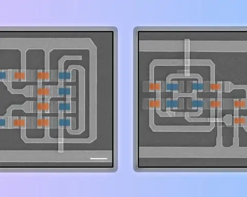
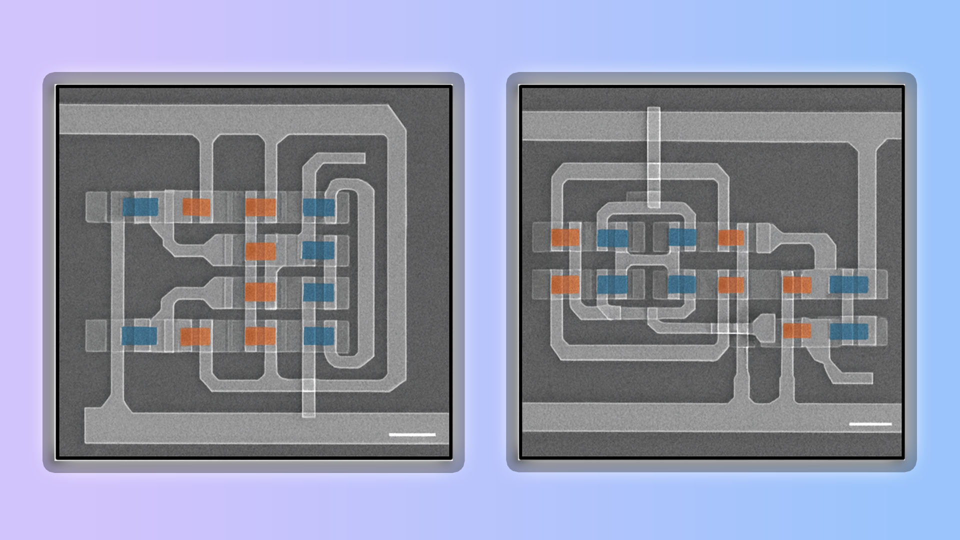
- Scale: >2,000 transistors in total were fabricated for the demonstration (over 1,000 of each type). ScienceDaily
- Performance today: Operates below 3 V, up to ~25 kHz, with picowatt‑range power and ~100 pJ switching energy—proof‑of‑concept efficiency, not speed. Nature
- Why it matters: It proves fully complementary 2D CMOS can be built and made to work at wafer scale—an essential step toward post‑silicon logic and ultra‑thin, low‑power electronics. psu.edu
- What’s next: The team reports ~95% functional yield on a 2‑inch sapphire wafer and projects multi‑GHz potential if parasitic capacitance is reduced; near‑term niches could include edge AI, neuromorphic, and flexible electronics. The Register
- Peer‑reviewed: Results published June 11, 2025 in Nature. Nature
The story behind the world’s first silicon‑free 2D CMOS computer
A first that actually matters: complementary 2D logic at scale
For years, researchers have shown isolated 2D transistors and small logic gates. What Penn State’s team has now crossed is the CMOS threshold—they integrated both n‑type and p‑type 2D field‑effect transistors into a working computing system without any silicon. That “both” is crucial, because modern digital electronics depend on complementary pairs to achieve high performance at low power. Here, MoS₂ supplies the n‑type devices and WSe₂ supplies the p‑type, each grown as large‑area films and then engineered so their threshold voltages line up to form robust logic. psu.edu
The team fabricated over a thousand transistors of each polarity using metal–organic chemical vapor deposition (MOCVD) and stitched them into functional CMOS circuits. This isn’t a few inverters on a lab bench; it’s a wafer‑scale demonstration that complementary 2D electronics can be made to work as an integrated system. psu.edu
What exactly did they build? A one‑instruction computer
Calling this a “computer” can mislead if you’re picturing a desktop CPU. The chip implements an OISC (one‑instruction set computer)—a minimalist architecture that proves Turing‑complete computation is possible with a single instruction (often a subtract‑and‑branch variant). OISCs are terrific testbeds for new device platforms because they exercise logic, control flow, and memory access without requiring millions of transistors. Penn State’s OISC runs below 3 V and reaches ~25 kHz, limited primarily by parasitic capacitances in the early integration. The trade‑off is intentional: prioritize energy per switch (down in the picowatt regime, ~100 pJ per transition) and functional CMOS behavior over raw clock speed. Nature
How they pulled it off
Three technical moves stand out:
- Wafer‑scale 2D growth (MOCVD). Growing large, uniform films of MoS₂ (n‑type) and WSe₂ (p‑type) enables hundreds to thousands of devices on the same wafer. psu.edu
- Threshold‑voltage and leakage tuning. Through channel scaling, high‑κ gate dielectrics, and post‑processing, the team aligned n/p thresholds, increased drive current, and cut subthreshold leakage—making true 2D CMOS logic practical at low voltages. Nature
- System‑level validation. They didn’t stop at gates: they assembled combinational and sequential logic into a working OISC, then benchmarked performance with a SPICE‑compatible model calibrated to experimental data. Nature
How “first” is this first?
In April 2025, another group reported a 32‑bit RISC‑V microprocessor built on 5,900 MoS₂ transistors, a notable leap in 2D integration. But that design did not demonstrate a silicon‑free, fully complementary 2D CMOS platform using both n‑ and p‑type 2D semiconductors. Penn State’s result is the first to realize a working CMOS computer made entirely of 2D materials, which is why the university—and Nature’s abstract—frame it as a distinct milestone. Think of the RISC‑V chip as breadth of integration with 2D devices, and Penn State’s OISC as depth in complementary 2D CMOS and system functionality without silicon. Nature
Performance now vs. potential later
Today’s ~25 kHz and sub‑3‑V operation won’t threaten silicon CPUs, but the energy profile is already compelling, and the path to speed is clear: reduce parasitic capacitances and push device scaling. In a follow‑up interview, the team cited ~95% functional yield across a 2‑inch sapphire wafer, and simulations suggest that with parasitics tamed, gate delays ~200 ps (~5 GHz) could be attainable—an aggressive but not unimaginable target as materials, contacts, and interconnects mature. The Register
Why 2D materials change the game
2D semiconductors maintain their properties at atomic thickness, mitigating short‑channel effects that bedevil ultra‑scaled silicon, and they invite novel stacking and integration schemes (including monolithic 3D) because layers can be assembled without the crystal‑lattice constraints of bulk materials. These attributes point to ultra‑thin, low‑power logic and potentially new system architectures where sensing, memory, and compute co‑locate in space. psu.edu
Realistic near‑term uses
Even before multi‑GHz 2D logic arrives, the demonstrated CMOS compatibility, low power, and extreme thinness make the platform attractive for specialized, resource‑constrained domains—think edge AI accelerators, neuromorphic hardware, and flexible/wearable systems where energy and form factor matter more than raw clock speed. That’s where Penn State’s team expects early traction. The Register
Who did the work, where, and when
The research—led by Saptarshi Das with first author Subir Ghosh—relied heavily on Penn State’s 2D Crystal Consortium–Materials Innovation Platform, part of the university’s Materials Research Institute ecosystem. The paper, “A complementary two‑dimensional material‑based one instruction set computer,” appeared in Nature on June 11, 2025. Funding came from the U.S. NSF, Army Research Office, and Office of Naval Research. psu.edu
What to watch next
- Parasitics & interconnects. Expect rapid progress on contacts, dielectrics, and wiring to boost speed while preserving the power advantage. Nature
- Scale & yield. The reported wafer‑level yields are encouraging; automating alignment and transfer steps is the next industrial hurdle. The Register
- System complexity. Moving from an OISC to richer instruction sets and on‑chip memory will test variability control and design libraries for 2D CMOS. The Register
- Context in the field. Parallel advances—like the MoS₂‑based 32‑bit RISC‑V prototype—show that 2D logic is scaling fast on multiple fronts. Nature
Bottom line
Penn State’s device isn’t “the end of silicon” yet—but it is the first fully 2D, silicon‑free CMOS computer to cross the finish line in peer‑reviewed literature. That makes it a genuine landmark: it validates the materials, processing, and circuit techniques needed for complementary 2D logic at wafer scale, and it charts a credible path toward ultra‑thin, ultra‑efficient electronics that we simply can’t build with bulk silicon. psu.edu
Sources
Penn State news release; Nature paper and abstract; ScienceDaily and SciTechDaily summaries; coverage and quotes in The Register interview; and background on OISC. Wikipedia